- wusheng888@126.com
- Monday-Friday:09:30 pm-05:00pm
- Address: Unit 1111, 11/F, Hollywood Plaza, 610 Nathan Road, Mongkok, Kowloon, HongKong.

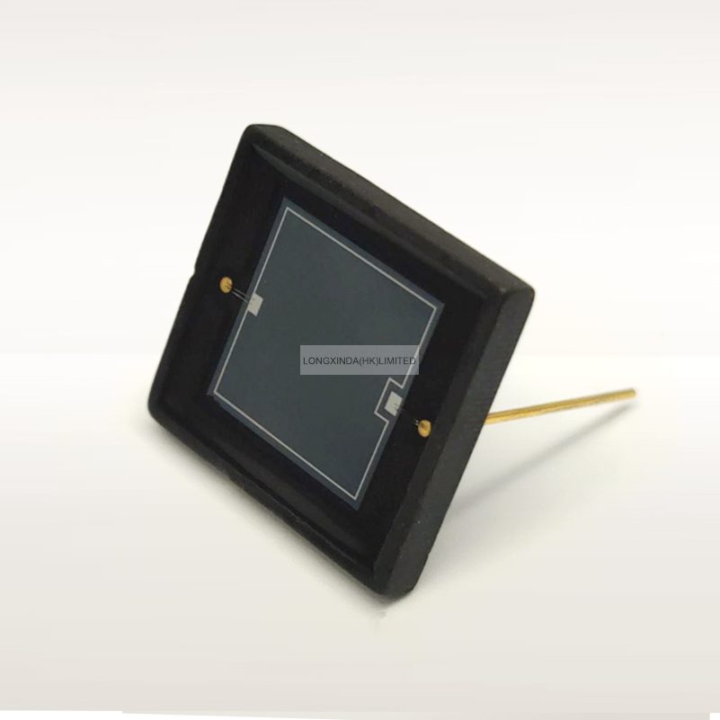
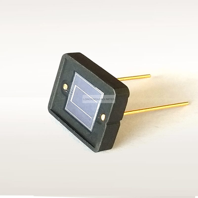
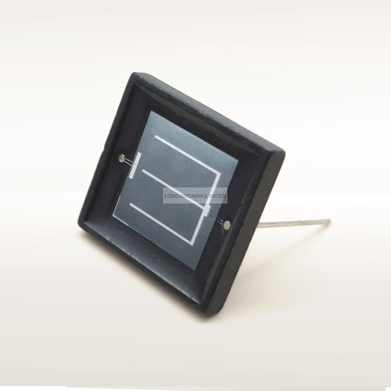
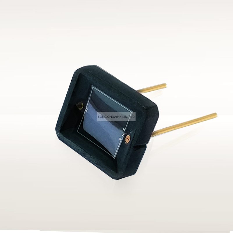
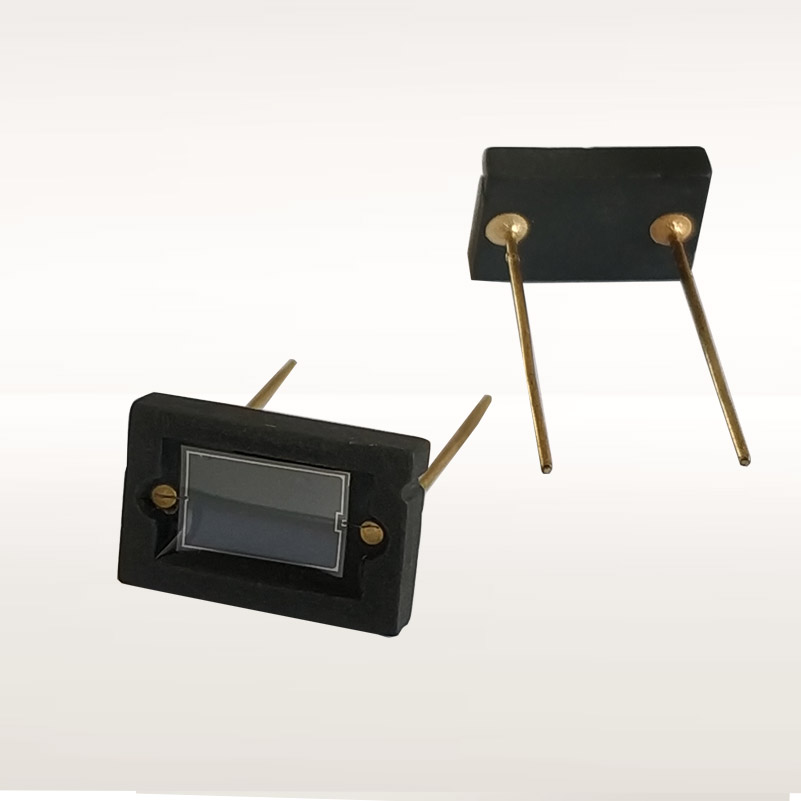
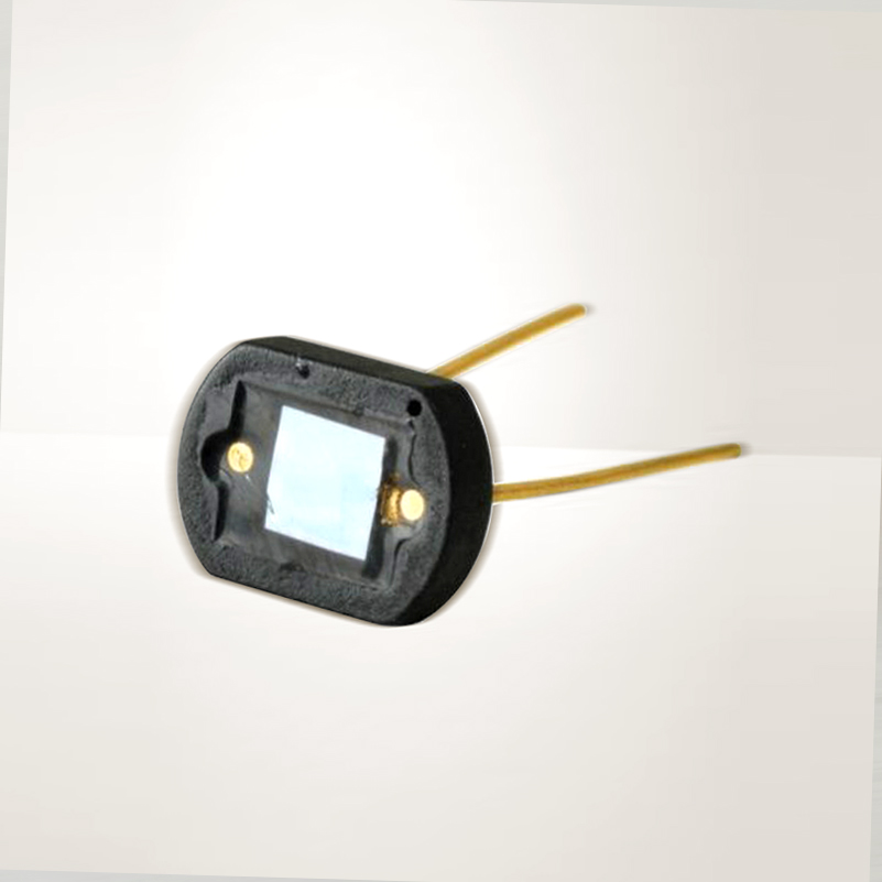
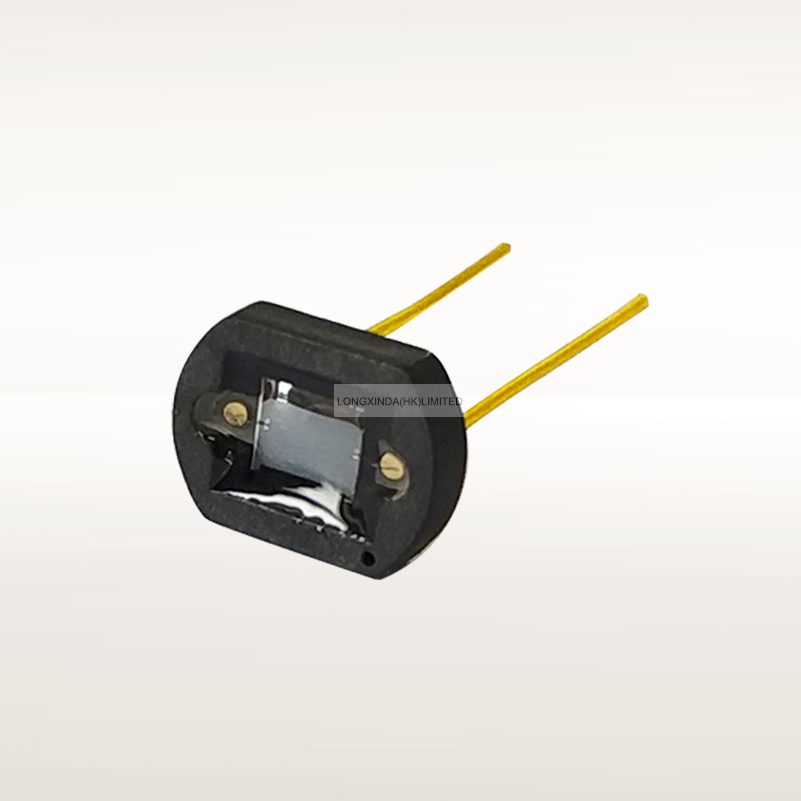
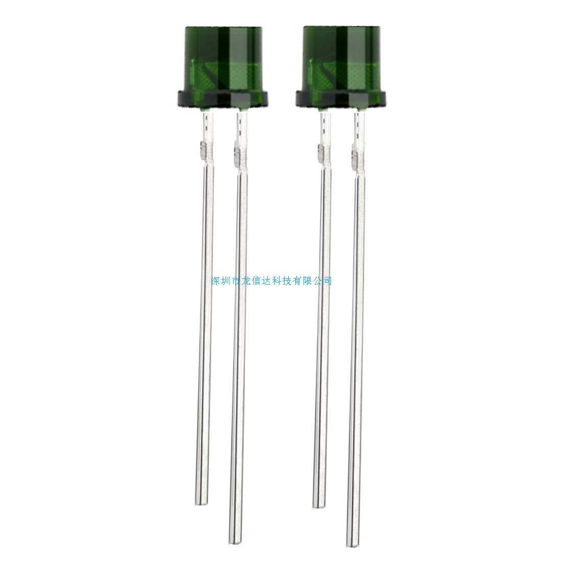
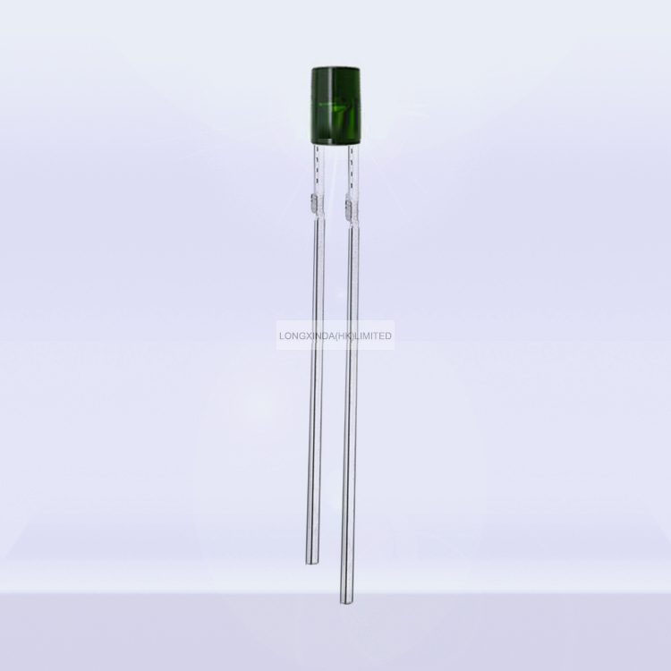
Optocouplers (Photocell (CdS) Output)
The CdS photocell output optocouplers optically couple an LED to a CdS Light Dependent Resistor (LDR). The LDR resistance increases when the LED current is OFF and decreases when LED current is ON. The device showcases a large dynamic range with a response time that efficiently mimics the human eye's sensitivity to light changes. Engineered with High, Medium, and Low dark resistances, the optocouplers are available with diverse resistance values to suit various applications. The photocells are encased in an opticallyisolated structures.
Type No.: NSL-37V55
10KΩ ON-Resistance Photocell (CdS) Output Optocoupler
The NSL-37V55 is an optocoupler that has an OFF-resistance of 1MΩ.
■Typical Applications:
● Industrial
● Audio Compressors
● Electrical Noise Filter
■Features
● Compact Moisture Resistant Package
● Low LED Current
● Very Low “On” Resistance
●Passive Resistance Output
●Low Distortion
| Parameter | Symbol | Min | Max | Unit |
|---|---|---|---|---|
| Isolation Voltage | IF | - | 2500 | V |
| Operating Temperature | VF | -40 | +85 | °C |
| Storage Temperature | VR | -40 | +85 | °C |
| Package | — | Plastic | — | — |
| Parameter | Test Conditions | Symbol | Min | Typ | Max | Unit |
|---|---|---|---|---|---|---|
| Forward Current | - | IF | - | - | 40 | mA |
| Forward Voltage | IF=20mA | VF | - | - | 2.5 | V |
| Reverse Voltage | - | VR | - | - | 3.0 | V |
| Parameter | Test Conditions | Symbol | Min | Typ | Max | Unit |
|---|---|---|---|---|---|---|
| Maximum Photocell Voltage | Peak AC or DC | VC | - | - | 100 | V |
| Power Dissipation¹ | - | PD | - | - | 175 | mW |
| Parameter | Test Conditions | Symbol | Min | Typ | Max | Unit |
|---|---|---|---|---|---|---|
| On-Resistance | IF=1mA | Ron | 10 | - | 30 | kΩ |
| Off Resistance | 10 sec after IF=0mA | Roff | 1 | - | - | MΩ |
| Rise Time | Time to 63% of final conductance @ IF=2.0mA | TR | - | 3.5 | - | msec |
| Decay Time | Time to 1MΩ | TF | - | - | 500 | msec |
¹Derate linearly to 0 at 75 °C. ²The Rise Time, /(T_R/), is the time required for the dark to light change in conductance to reach 63% of its final value.
■Typical Mechanical Specifications
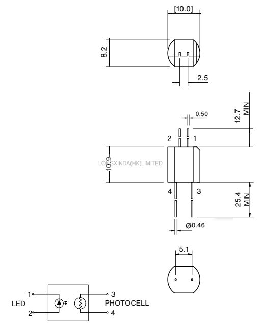
Units are in [mm] The product has tolerances.
■General Care and Handling Instructions
Handling and Storage
• Handle Optocouplers and LEDs gently to prevent damage.
• Avoid exposing the devices to temperatures exceeding the storage temperature rating of the device.
• Maintain a non-condensing environment for optimum performance and lifetime.
Cleaning
• For plastic molded devices, cleaning with a 50/50 mixture of Methanol and isopropyl alcohol is recommended. Cleaning in an ultrasonic bath is generally not recommended.
Special Considerations
• Avoid exposing plastic molded devices or epoxy glob topdevices to harsh chemicals like THINNERS, ACETONE, andTRICHLOROETHYLENE.
■Legal Disclaimer
Information in this data sheet is believed to be correct and reliable. However, no responsibility is assumed for possible inaccuracies or omission. Specifications are subject to change without notice.
不能為空
E-mail格式不對
不能為空