- wusheng888@126.com
- Monday-Friday:09:30 pm-05:00pm
- Address: Unit 1111, 11/F, Hollywood Plaza, 610 Nathan Road, Mongkok, Kowloon, HongKong.

1. Scope :
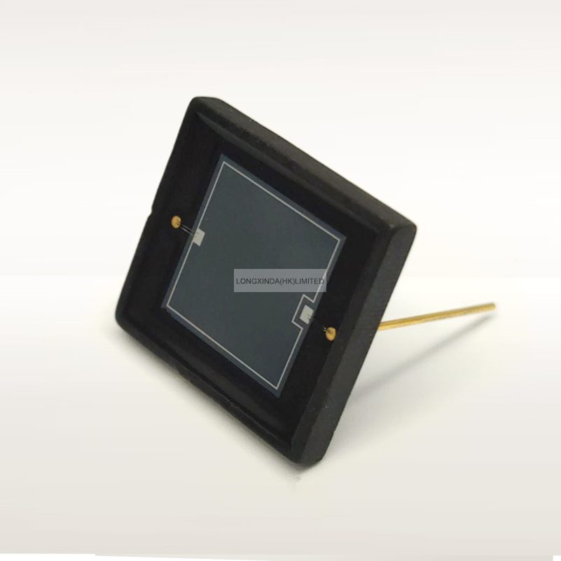
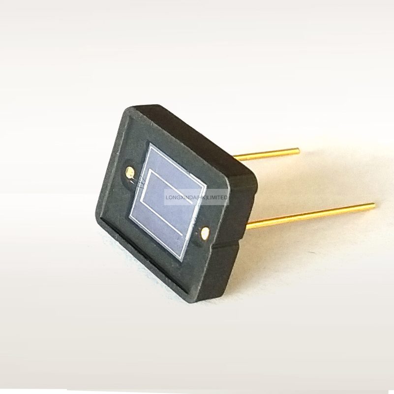
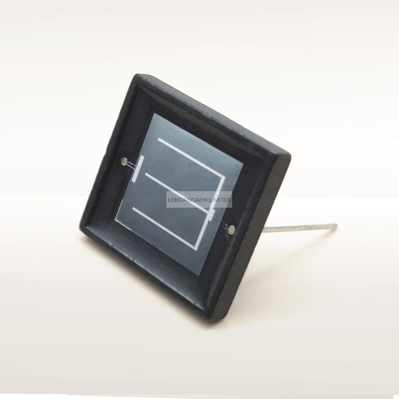
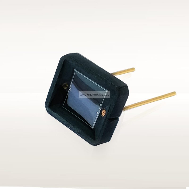
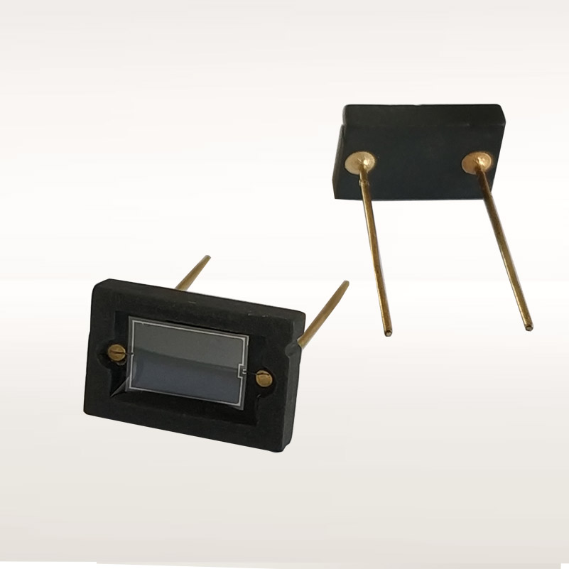
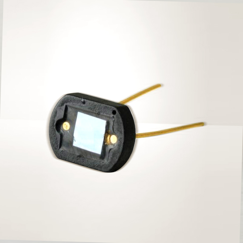
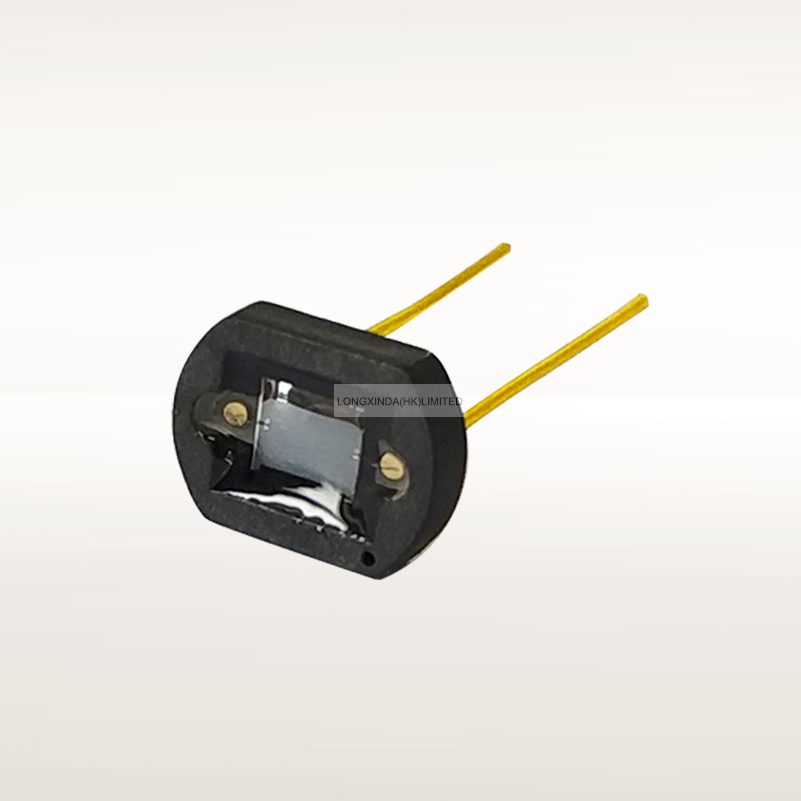
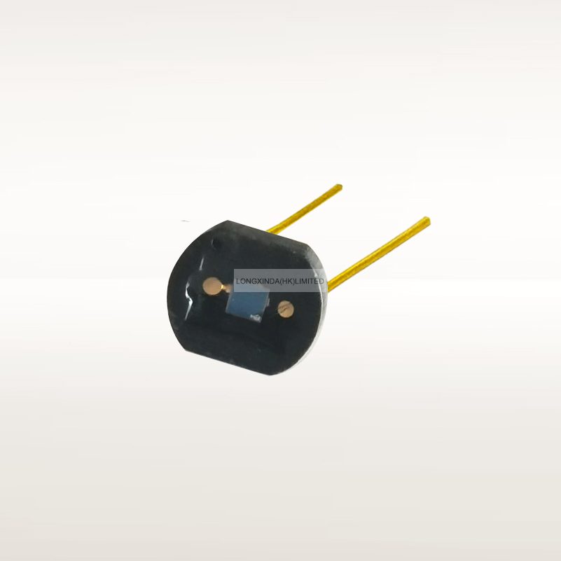
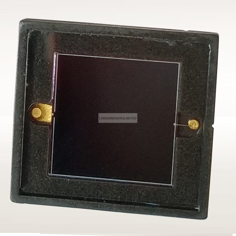
This specification applies to PN silicon photodiode chips,
Device NO. LXD-PN06085
Structure :
2-1. Planar type : PIN diode.
2-2. Electrodes :
Top side (Anode
) : Aluminum alloy . Back side (Cathode ) : Gold alloy .
3. Size :
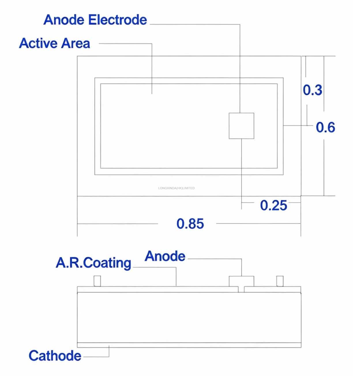
3-1. Chip size : 23.6 mils x 33.5 mils (0.60 mmx0.85 mm ).
3-2. Chip thickness : 8.6 x 1.2 mils (0.220x0.030mm ).
3-3. Active area : 17.7 mils x 27.6 mils (0.45 mm 0.70 mm ).
3-4. Bonding pad (Anode ) : 4 mils x 4mils (0.10mm 0.10 mm) .
3-5. Pattern drawing : Refer to the attached drawing.
Electro-optical characteristics (Ta = 25 )
| Parameter | Symbol | Condition | Min. | Typ. | Max. | Unit |
|---|---|---|---|---|---|---|
| Reverse light current | IL | V_R=5V, T=2856K, Ee=5mW/cm² | 2 | — | — | μA |
| *Reverse dark current | ID | V_R=5V, Ee=0mW/cm² | — | — | 10 | nA |
| *Reverse breakdown voltage | V(BR)R | I_R=100μA, Ee=0mW/cm² | 50 | — | — | V |
| *Forward voltage | VF | I_F=100mA | — | 1.3 | 1.5 | V |
| Total capacitance | Ct | V_R=5V, Ee=0mW/cm², f=1MHz | — | 3.5 | — | pF |
| Responsivity | Rφ | V_R=10V, λ=880nm | — | 0.50 | — | A/W |
| Responsivity | Rφ | V_R=10V, λ=650nm | — | 0.3 | — |
A/W |
* Based on 100% probing
Plsease input value
Error E-mail format
Plsease input value