- wusheng888@126.com
- Monday-Friday:09:30 pm-05:00pm
- Address: Unit 1111, 11/F, Hollywood Plaza, 610 Nathan Road, Mongkok, Kowloon, HongKong.

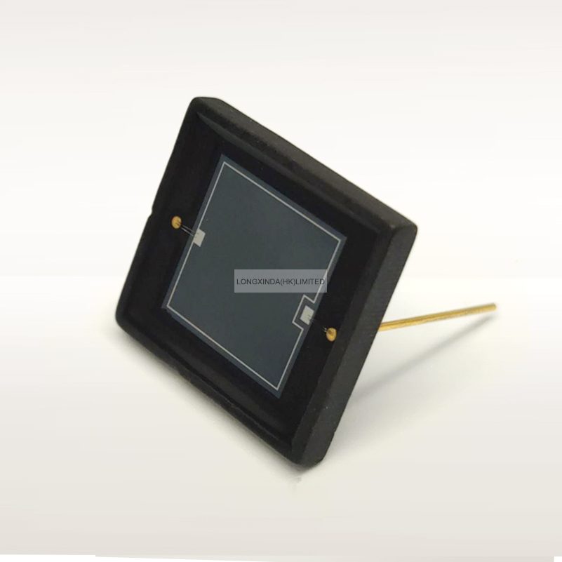
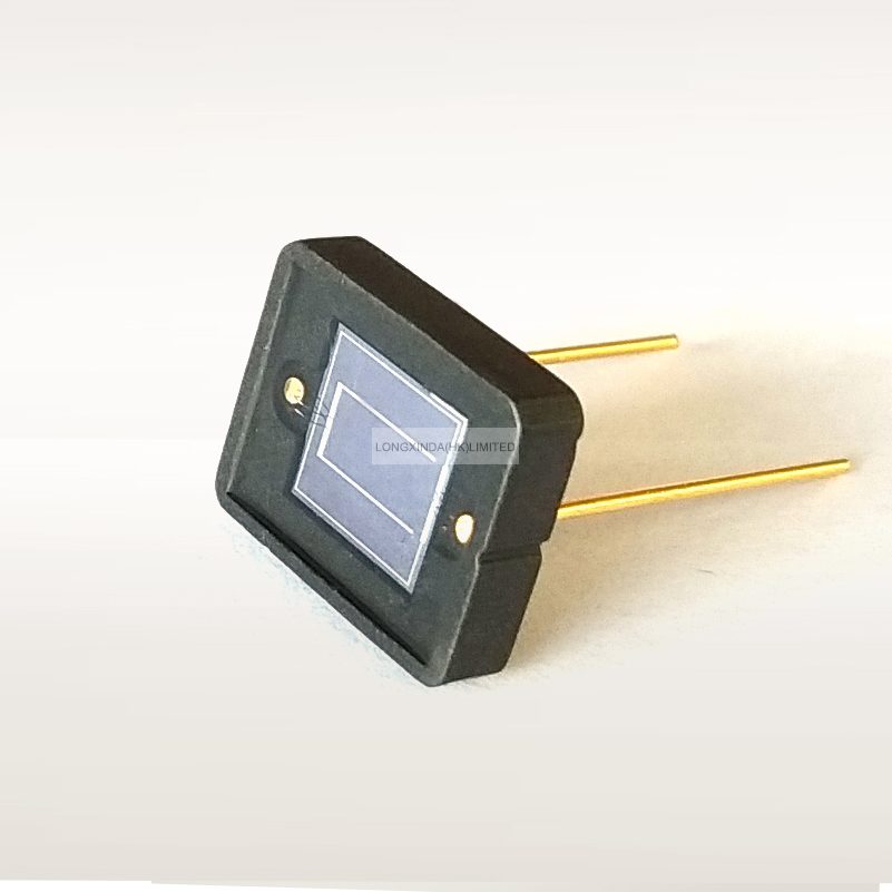
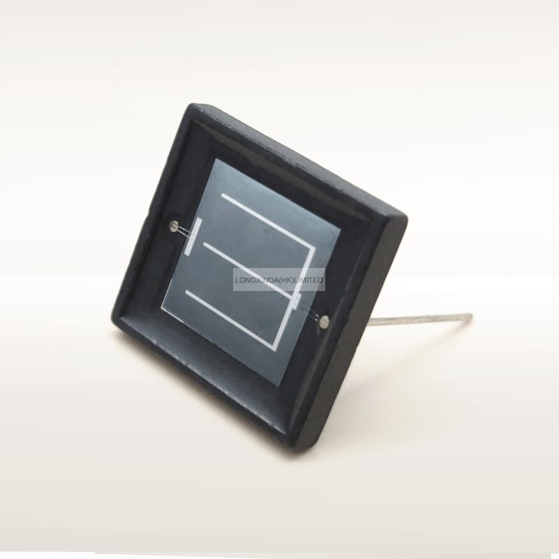
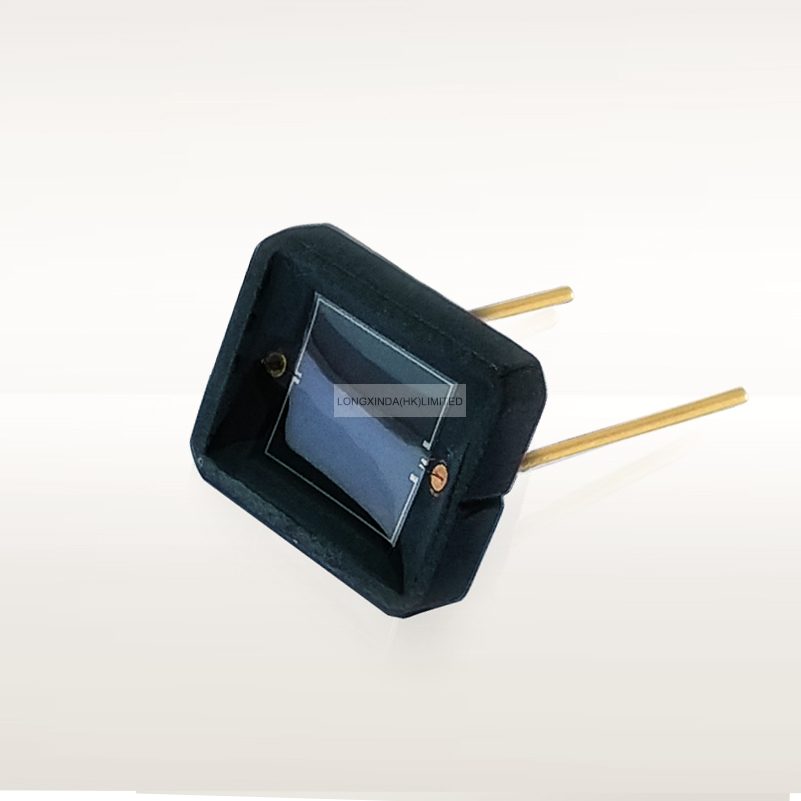
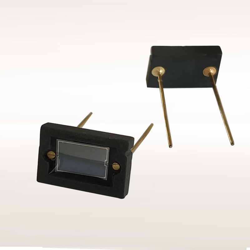
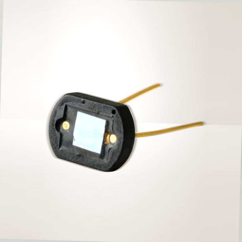
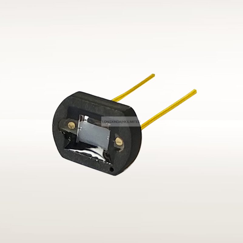
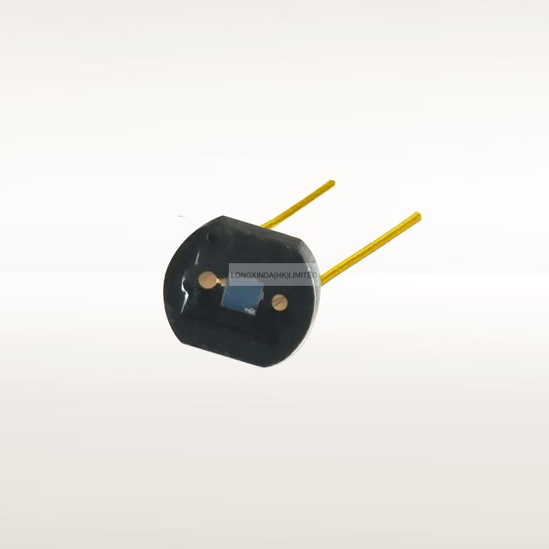
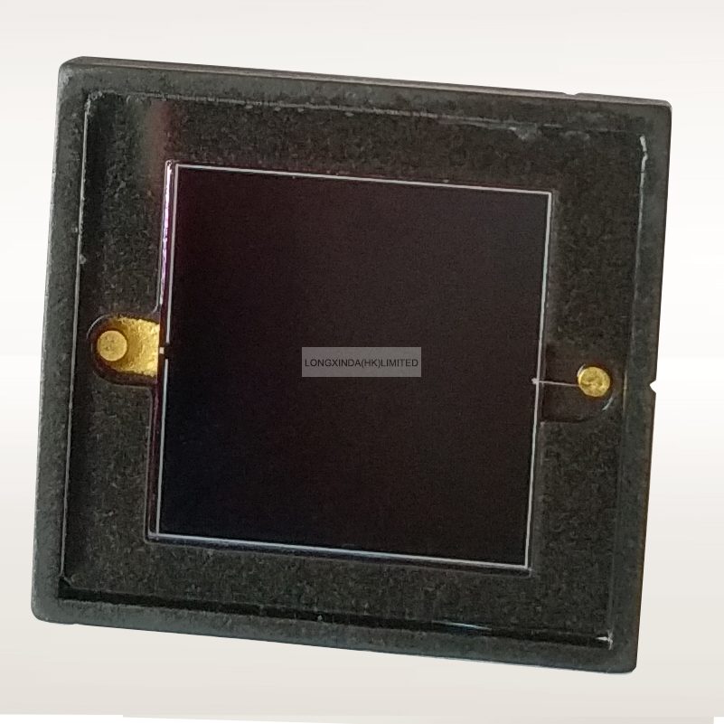
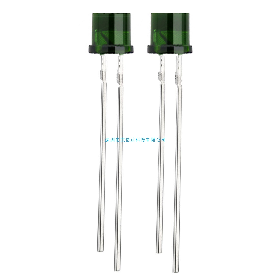
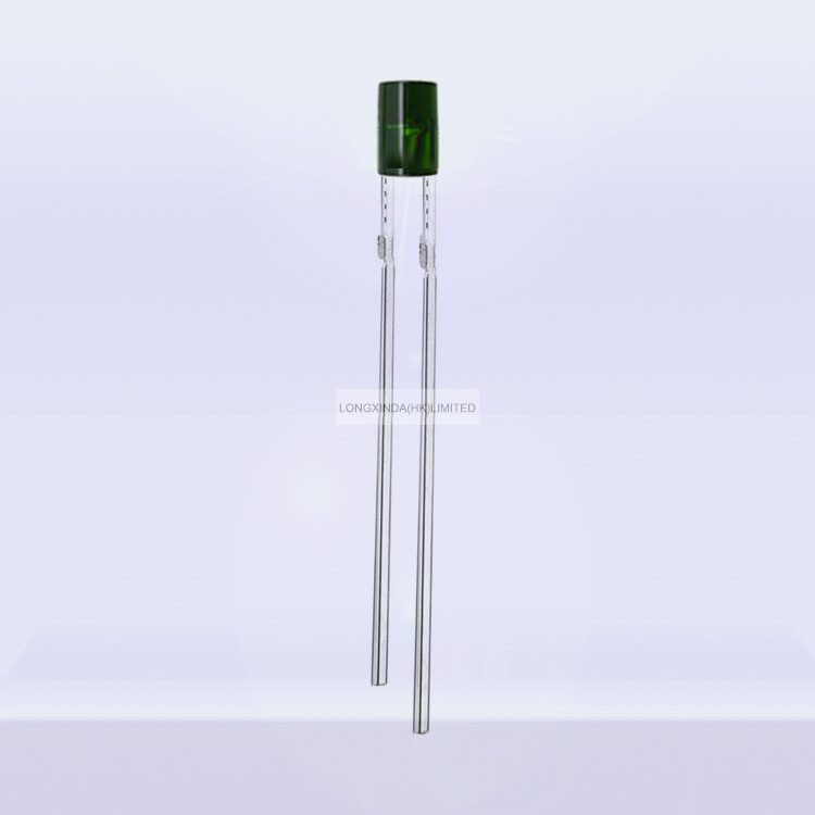
This is an overview of 393.70 x 393.70 mil silicon photodiode chips. We can assist customers in technology development by providing 3-inch (traditional diffusion process) or 6-inch (particle injection process) silicon wafer plate drawings or customized designs, helping customers in the field of optoelectronic detection with technology research and development, related new product derivatives, and scientific research. We retail chips or provide you with finished products in different packaging forms, such as TO metal, ceramic SMT、 Arrays and modules, etc.
1. Scope :
This specification applies to PIN silicon photodiode chips.
Device No: LXD-PN1008
2. Structure :
2-1. Planar type : PIN diode.
2-2. Electrodes :
Top side (Anode ) : Aluminum alloy .
Back side (Cathode ) : Gold alloy .
3. Size :
3-1. Chip size : 394 mils × 354 mils (10.008 mm × 8.992 mm)
3-2. Chip thickness : 12 ± 1.5 mils (0.305 ± 0.038 mm )
3-3. Active area : 315 mils × 315 mils (8.001 mm × 8.001 mm)
3-4. Bonding pad :
Anode: 70.1 mils × 10.2 mils (1.781 mm × 0.259 mm)
Cathode: 30.4 mils × 10.39 mils ( 0.772 mm × 0.264 mm)
3-5. Pattern drawing : Refer to the attached drawing.
4. Electro-optical characteristics (Ta = 25℃)
| Parameter | Symbol | Condition | Min. | Typ. | Max. | *Unit |
| *Reverse dark current |
ID | VR=5V Ee=0mW/cm² |
100 | nA | ||
| *Open circuit voltage |
Voc | T=2856K Ee=5mW/cm² |
350 | mV | ||
| Reverse Voltage |
V(BR)R | IR=100PA Ee=0mW/cm² |
10 | V | ||
| Total Capacitance |
CT | VR =0V Ee=0mW/cm² f=1MHz |
720 | pF | ||
| Short circuit Current |
Isc | VR =0V Ee=5mW/cm² T=2856K |
675 | PA |
*Based on 100% probing
不能為空
E-mail格式不對
不能為空