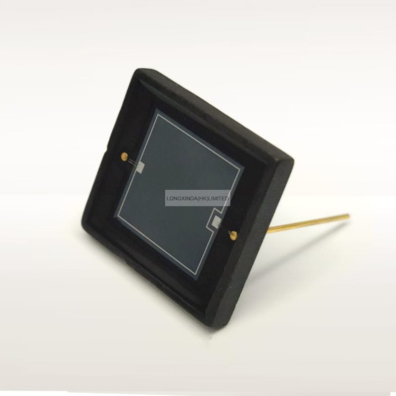
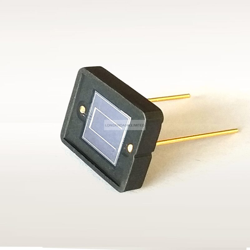
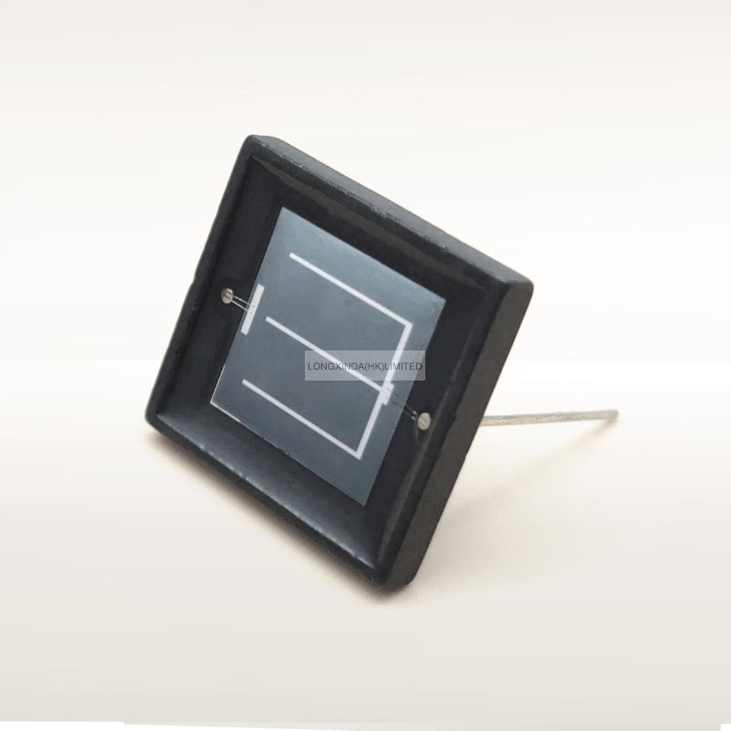
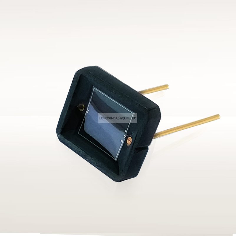
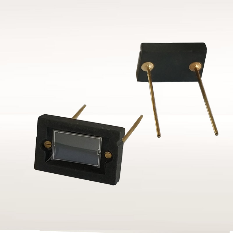
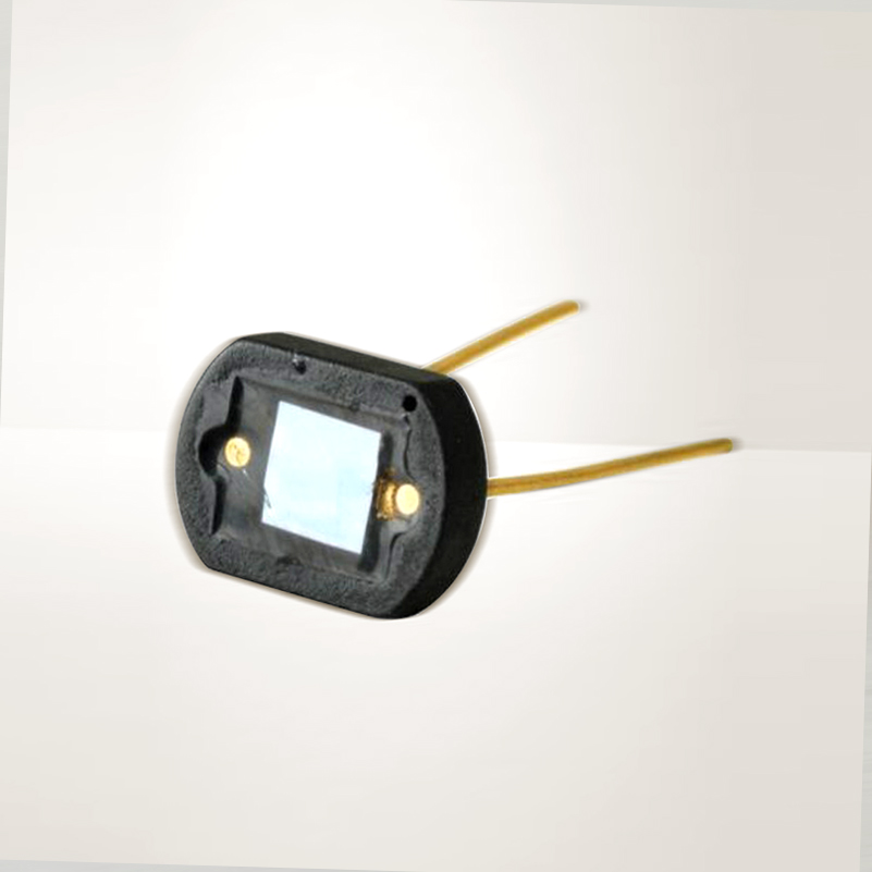
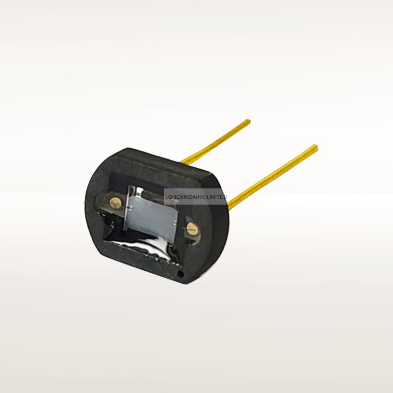
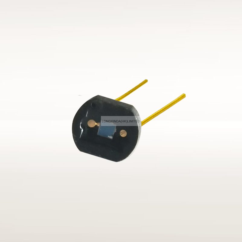
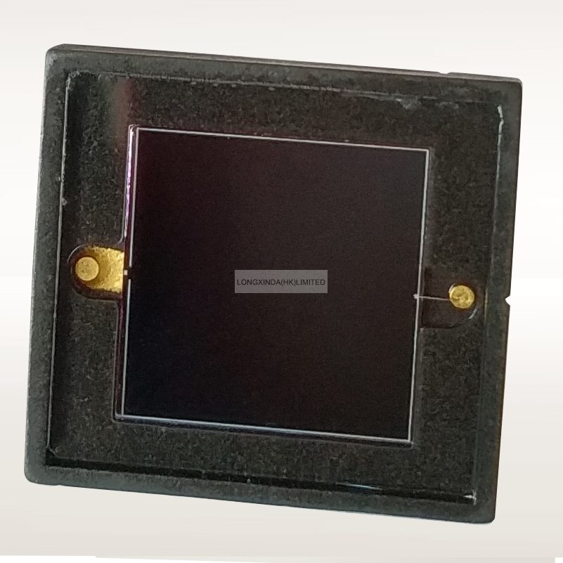
3.0x3.0mm SILICON PHOTODIODES CHIP LXD-PIN33
Подробная информация
Запрос
grade PIN Silicon Photo-diode Chip Specification
1. Scope
- The specification applies to PIN silicon photo-diode chips.
- Type : LXDPIN120-G.
2. Structure
- PIN planar type.
- Electrode topside (anode) : Aluminum.
- Electrode backside (cathode) : Gold.
3. Size
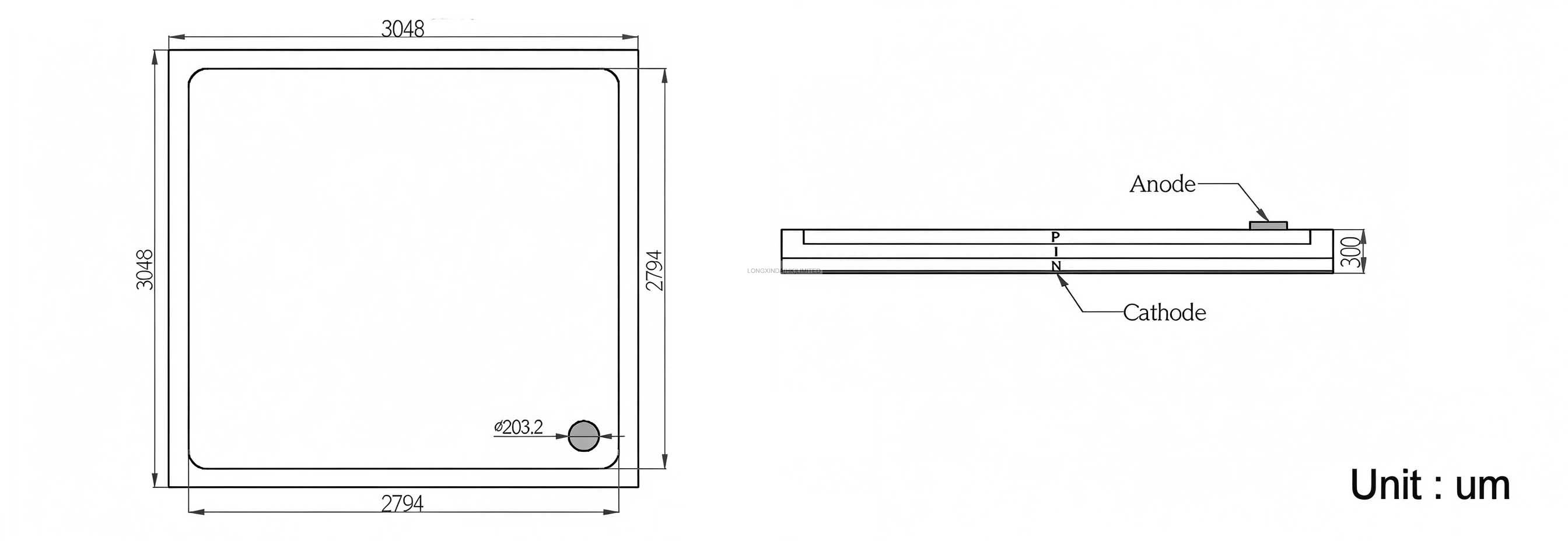
- Chip size (including scribe lane) : 120.0mil × 120.0mil (3.048mm × 3.048mm)
- Die size : 118.8mil × 118.8mil ± 0.6mil (3.018mm × 3.018mm ± 0.015mm)
- Thickness : 11.8mil ± 1mil (0.300mm ± 0.025mm)
- Active area : 110.0mil × 110.0mil ± 0.5mil (2.794mm × 2.794mm ± 0.013mm)
- Pad size : Diameter 8mil ± 0.4mil (0.203mm ±0.01mm )
- Pattern drawing : per fig. 1
4. Electro-Optical Characteristics(Ta=+25℃)
| Parameter |
Symbol |
Condition |
Min. |
Typ. |
Max. |
Unit. |
| Forward Voltage |
VF |
IF=10mA, H=0 |
0.5 |
— |
1.3 |
V |
| Reverse Breakdown Voltage |
VBR |
IR=100μA, H=0 |
35 |
— |
— |
V |
| Reverse Dark Current |
ID |
VR=10V, H=0 |
— |
— |
10 |
nA |
| Light Current |
IL |
VR=5V, H as 1mW/cm²@940nm |
— |
162 |
— |
μA |
| Junction Capacitance |
CJ |
VR=3V, Vac=0.1V, H=0, F=1MHz |
— |
44 |
— |
pF |
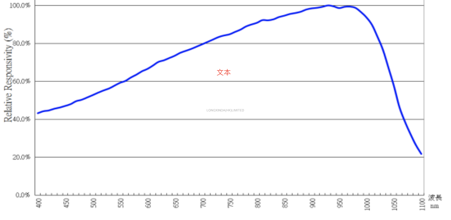
| Peak Sensing Wavelength |
λP |
— |
— |
940 |
— |
nm |
Fig.1 Pattern Drawing Description